Pioneering new frontier of
ultra-wide band gap semiconductors
Driving aluminum nitride–based semiconductor technologies
Bring cutting-edge devices to the world
What’s New
-

Exhibition at Photonics West
ULTEC exhibited its deep-ultraviolet laser diodes at the SPIE Photonics West Exhibition, held from January 17 to 22, 2026. During the exhibition, we had the pleasure of welcoming a large number of visitors with strong interest in our deep-ultraviolet laser diodes. We engaged in active and wide-ranging discussions on potential applications, considerations for business implementation, … Read more
-
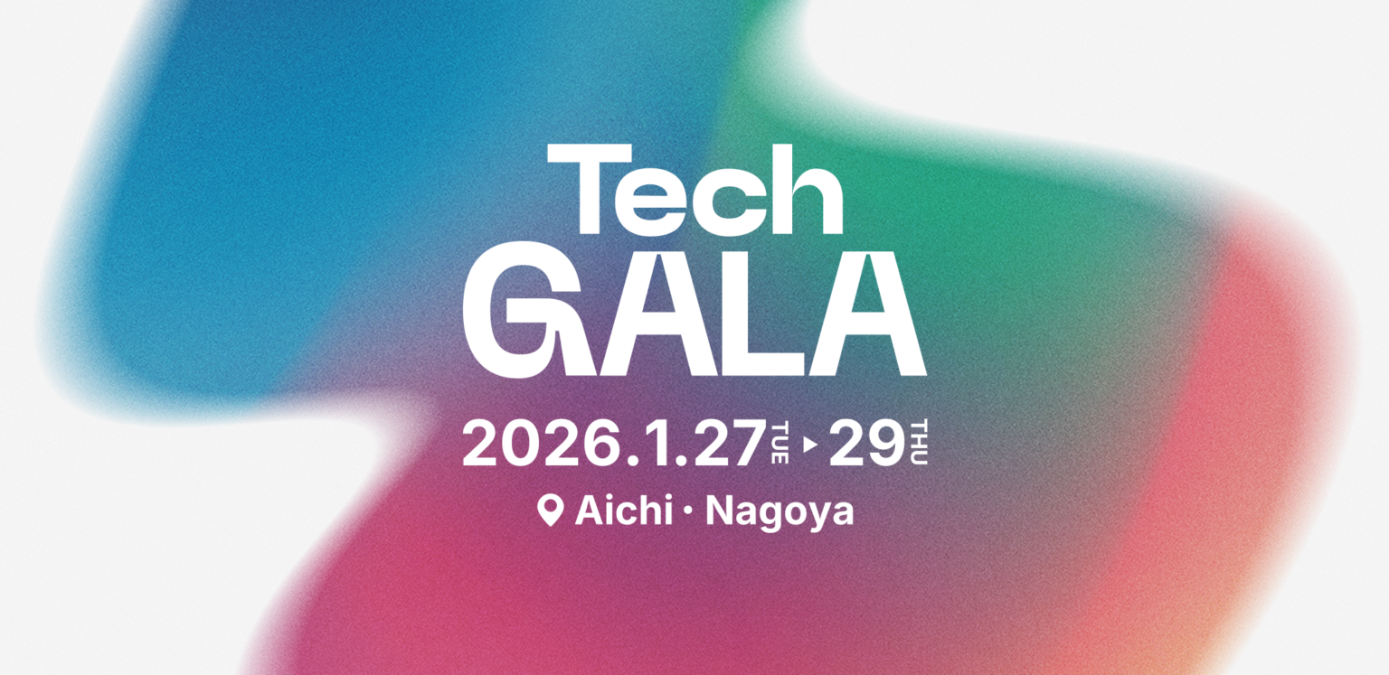
Ventures Talk 2026
Dr. Akira Yoshikawa, President and CEO of ULTEC, delivered a talk at Ventures Talk 2026 – A Gathering of Venture Companies Originating from Tongali Academia. This event was held as one of the official programs of TechGALA, a technology festival dedicated to shaping the future of our planet. Through this valuable speaking opportunity, we were … Read more
-
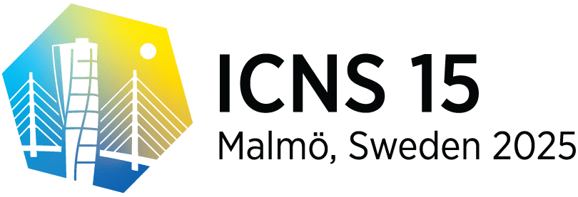
Plenary Talk in ICNS-15
Dr. Maki Kushimoto, Technical Advisor to ULTEC, gave a plenary talk at the 15th International Conference on Nitride Semiconductors (ICNS-15), one of the premier international conferences on nitride semiconductors. In this plenary talk, we reported the world’s first continuous-wave operation in the UVB wavelength range of 280–300 nm, achieved through a collaborative research effort between … Read more
-
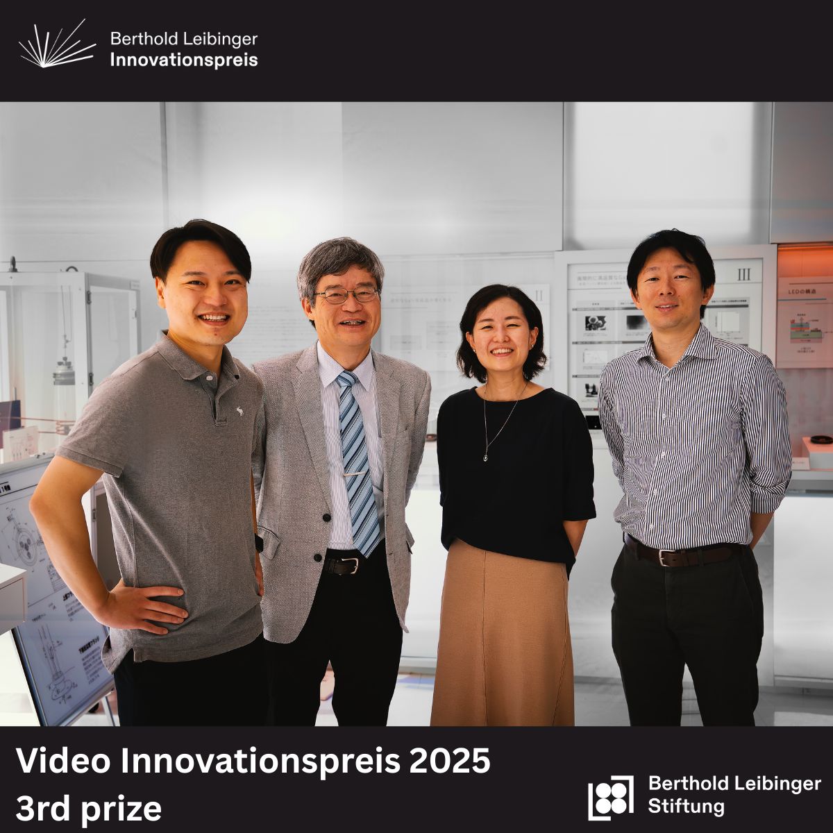
Berthold Leibinger Innovationspreis
We are excited to announce that on June 20, 2025, ULTEC was awarded third prize at the prestigious Berthold Leibinger Innovationspreis for its cutting-edge Deep-UV laser diode technology. The realization of blue LEDs and laser diodes—once deemed impossible—transformed the world by revolutionizing lighting and display technologies. Today, researchers continue to push the boundaries of photonics, aiming for even shorter wavelengths. Among the most ambitious … Read more
-
ULTEC Recognized as a Nagoya University Certified Startup
We are pleased to announce that ULTEC Inc. has been officially certified as the 88th Nagoya University Certified Startup, effective May 1, 2025. This recognition is awarded to startups founded on intellectual property developed at Nagoya University, and marks our commitment to bridging cutting-edge academic research with real-world applications as a university-originated venture. University-certified startups play a key role … Read more
-

Exhibit at Startup JAPAN
We are excited to announce that ULTEC will be exhibiting at Startup JAPAN 2025, one of the largest startup exhibitions in Japan, taking place in 2025. ■ Event Details• Event Name: Startup JAPAN 2025• Date: May 8 (Thu) – May 9 (Fri), 2025• Venue: Tokyo Big Sight, Koto-ku, Tokyo• Official Website: https://eight-event.8card.net/climbers/startup-japan/ We look forward … Read more
ULTEC Inc.
TOIC NAGOYA, Furo-cho, Chikusa-ku, Nagoya, Aichi 464-0814, Japan